- Products
- Products
- Companies
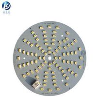
Golden Supplier ceramic substrate printed board bcp pcb design for electronics product

-
Supplier: Kinglisheng(Shenzhen) Electronics& Technology Co., Ltd. -
Region: Guangdong, China -
Contact: Ms Essie Mei -
Price: $0.10 /piece -
Min. Order: 1 piece
Product details
| Certificate: | UL, CQC, TS16949, ISO14000, ROHS; | Brand Name: | KLS; |
| Layer count: | 1-32layers; | Min. Line Width: | 0.1mm; |
| Min. Line Spacing: | 0.1mm; | Board Thickness: | 0.1mm-3mm; |
| Surface Finishing: | HASL,Immersion Gold,OSP, Immersion Silve, Electrolytic gold; | Min. Hole Size: | 0.1mm; |
| Key Words: | ceramic pcb; | Model Number: | ceramic pcb; |
| Packaging Detail: | Vacuum plastic bag and carton for Trade Assurance Factory professional OEM ceramic pcb; | Number of Layers: | 4-Layer; |
| Base Material: | Al2O3, AIN; | Product name: | Trade Assurance Factory professional OEM ceramic pcb; |
| Application: | Electronics Device; | Solder mask color: | Green,black,Blue,White,Yellow,Red; |
| Port: | Shenzhen; | Place of Origin: | Guangdong China (Mainland); |
| Outline: | Routing,V-Groove, Beveling punch; | Silkscreen colour: | White,Yellow,Red,Black; |
| Supply Ability: | 10000 Cubic Meter/Cubic Meters per Month; | Service: | One-stop Service; |
| Testing Service: | IPC-600 II; | Payment Terms: | L/C,D/A,D/P,T/T,Western Union,MoneyGram; |
| Copper Thickness: | 0.5 OZ-4 OZ; | Delivery Detail: | Shipped in 5 days after payment; |
Product Description
Golden Supplier ceramic substrate printed board bcp pcb design for electronics product
Product Detail
| Layer count | 1-32layers |
| Solder mask color | Green,black,Blue,White,Yellow,Red |
| Silkscreen colour | White,Yellow,Red,Black |
| Outline | Routing,V-Groove, Beveling punch |
| Certificate | UL, CQC, TS16949, ISO14000, ROHS |
| Product name | Trade Assurance Factory professional OEM ceramic pcb |
| Key Words | ceramic pcb |
| Application | Electronics Device |
| Service | One-stop Service |
| Testing Service | IPC-600 II |
| Product Keywords | ceramic substrate printed board bcp,ceramic substrate pcb design |
Product Category

Company Information

Our Advantages
Certifications

FAQ
Packaging & Shipping

Packaging
Payment
Fast Delivery
Different amount of time will be required for differentContact Us
 Go to homepage
 VIEW MORE
You may like
-
Manufacturing custom design multi -layer HDI PCB and PCBA assembly plants for medical equipment for medical equipment

-
One Stop PCB Service Printed Circuit Factory Custom Multilayer PCBA Board All PCB Assembly and Manufacturing
-
Multilayer PCB Assembly Manufacturer ShenZhen Electronics SMT PCBA Factory
-
Shenzhen Customize PCB PCB Circuit Multilayer Pcb Manufacturer
-
Manufacturer PCB Circuit Board Assembly Professional Customer Printing Prototyping Factory Multilayer PCB and PCBA
-
Electronics Factory Multilayer Printed Circuit Board Manufacturer OEM ODM PCBA PCB Manufacturer Offer Electronic PCB Design
-
Original brand new TP.MS358.PB801 4-core wifi network 32--50 inch universal three-in-one motherboard suitable for smart TV accessories
-
Support one stop service Oem Professional Pcba Drone Pcb Drone Pcba
-
Cem-1 94v0 pcb schematic circuit board design services
-
Wind source dual system swimming pool heat pump constant temperature controller CC395 CCYCKB001


Other Products
-
$0.10 / piece
-
$0.10 / piece
-
PCB /PCBA design,bom list & gerber files, multilayer ,prototype PCB Customs Data Experienced Factory$0.10 / piece
-
$0.10 / piece
-
$0.10 / piece


Related Search
ceramic substrate printed board pcb
pcb design for fm transmitter pcb suppliers
molding machine for electronics product suppliers
ceramic substrate
aln ceramics substrate
aln ceramic substrate
metalized ceramic substrate
led ceramic substrate metalized
ce ceramic substrates high
oven for electron board suppliers