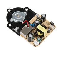
Multilayer pcb circuit board manufacturer 1~30 layers
-
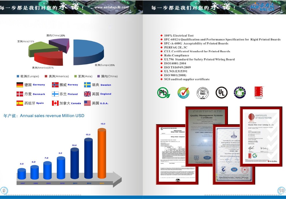
Supplier: Shenzhen Anlida Electronics Technology Co., Ltd. -
Region: Guangdong, China -
Contact: Mr Ken Zhang -
Price: $0.20 / 10 - 999 pieces
$0.15 / >=1000 pieces -
Min. Order: 10 pieces
Product details
| Minute line width: | 0.05mm/2mil | place of origin; place of origin: | Guangdong, China |
| product design: | Anlida Design | Shenzhen circuit board: | One-stop service |
| Minute line spacing: | 0.06 mm/2.5 million | Layers: | 1-40 floors, 12 floors |
| standard: | IPC-A-610G CLASS II&III | TG value: | T150-180 |
| Minute Hole Size: | 0.1mm/4mil | model: | M10-Y |
| Board Dimensions: | green/regular/red/black/yellow | brand: | Anli Dapu circuit board |
| product name: | ru 94VO printed circuit board | payment terms: | L/C, Western Union, D/P, D/A, T/T, MoneyGram, Paypal |
| Main services: | design manufacture assembly | Impedance Control: | 50/90/100±10% ohm |
| Types of: | multilayer board | Surface treatment: | ENIG OSP Sandblasting |
| Flame retardant: | 94v0 | Applications: | 94VO circuit board |
| Plate thickness: | 0.15-10mm | Substrate: | FR-4/PI/FR-4 High TG |
| Packaging Details: | Blister and carton and email: PCB design file, manufacturing file, DXF file, PAST file, Silk file, XY coordinate file. | Supply capacity: | 80000 square meters / month thick gold plating |
| port: | Shenzhen, China (Mainland) | Package preview: | |
| Copper thickness: | 0.25 oz - 12 oz |
Product Description
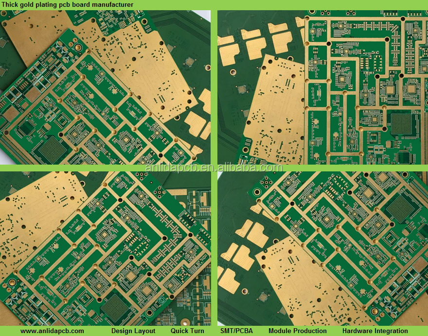
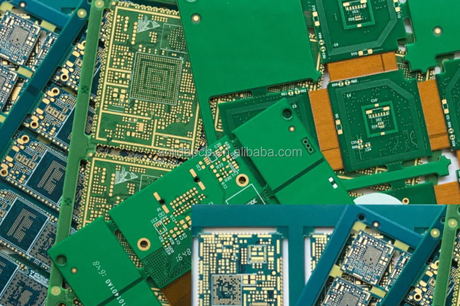
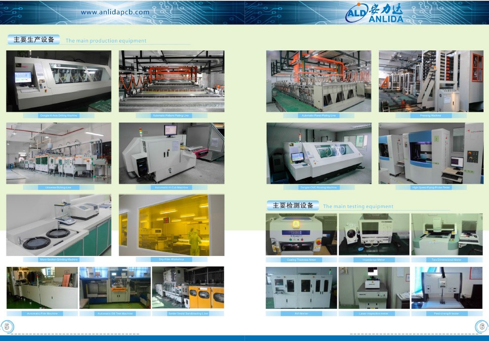
1~30 Layers Multilayer pcb circuit board manufacturer
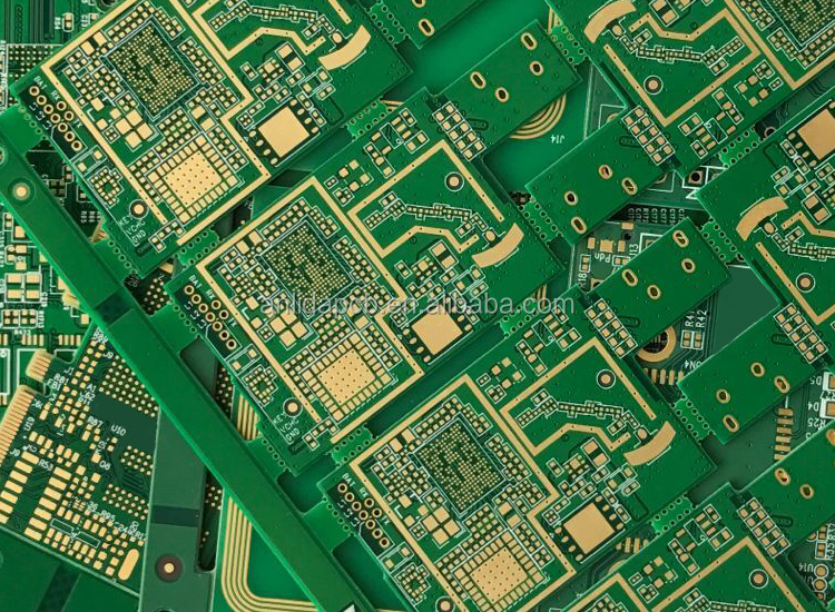
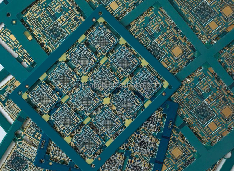
PCB product display:
All services:
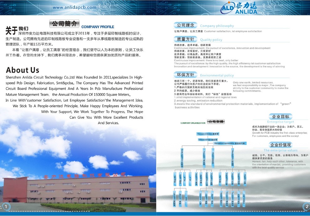
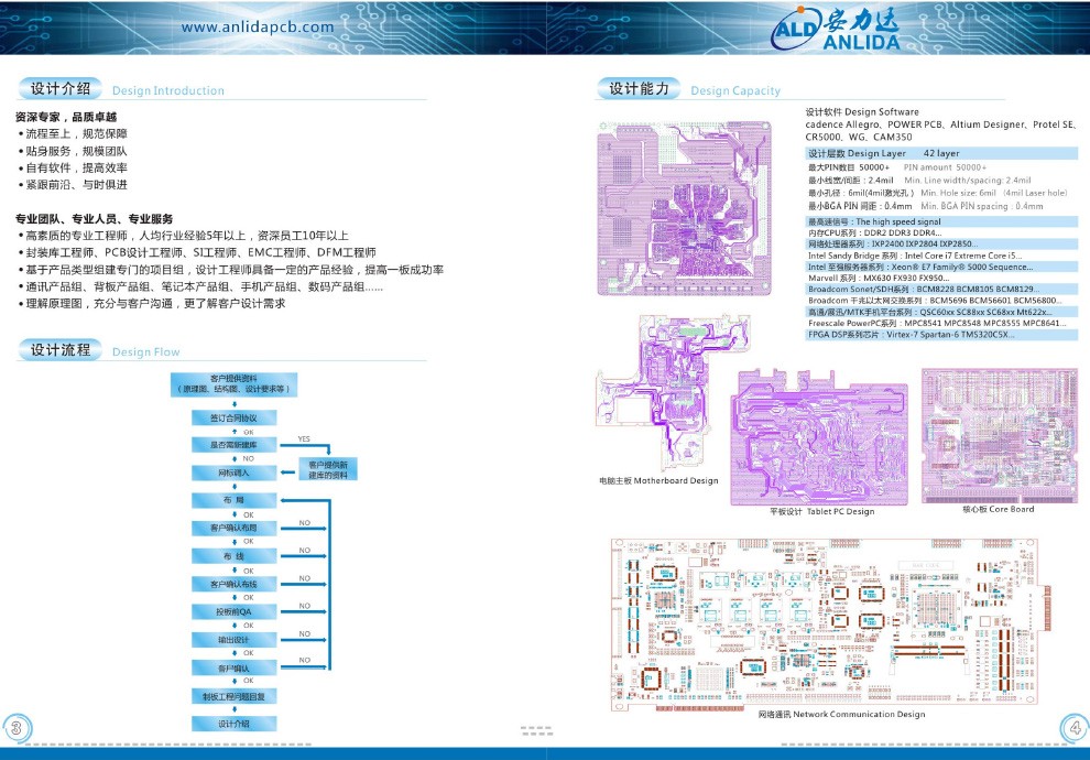
- High speed PCB design/PCB layout
- High speed PCB SI/PI/EMC analysis
- PCB reverse engineering design, engineering and early design support
- PCBA reverse engineering design
- Rapid 1-24LPCB prototyping, small to medium batch manufacturing
- Professional HDI PCB production
- Rigid-flex board manufacturing
- SMT assembly/PCBA assembly
- PCB parts procurement
PCB parameters:
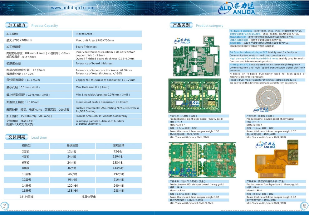
Printed circuit board production:
| Do not. | thing | prototype | mass production |
| 1 | layers | 1-30 floors | 1-20 floors |
| 2 | Maximum panel size | ≤1000X1000mm | ≤700X700mm |
| 3 | Substrate type | FR4, High Tg FR4, Rogers, Halogen Free | FR4, High Tg FR4, Rogers, Halogen Free |
| 4 | Maximum plate thickness | ≤10 mm | ≤10 mm |
| 5 | Minimum plate thickness | 2L≥0.2mm, 4L≥0.3mm 6L≥0.4mm, 8L≥0.6mm 10L≥0.65mm, 12L≥0.8mm |
2L≥0.2mm, 4L≥0.3mm 6L≥0.4mm, 8L≥0.6mm 10L≥0.65mm, 12L≥0.8mm |
| 6 | Minimum Line Width | ≥ 0.05mm(2mil) | ≥ 0.064mm (2.5 million) |
| 7 | Minimum line spacing | ≥ 0.064mm (2.5 million) | ≥0.075mm (3 million) |
| 8 | Minimum via | 0.15 mm (6 million) | 0.15 mm (6 million) |
| 9 | Minimum blind hole | 0.1 mm (4 million) | 0.1 mm (4 million) |
| 10 | Minimum Buried Via | 0.2mm (8 million) | 0.2mm (8 million) |
| 11 | Minimum Plated Hole Thickness | 20µm (0.8 million) | 20µm (0.8 million) |
| 12 | surface coating | HASL, ENIG, OSP, ENIG+OSP, electroplating Ni/Au/Ag | HASL, ENIG, OSP, ENIG+OSP, electroplating Ni/Au/Ag |
| 13 | Solder mask color | Green, blue, black, white, yellow, red | Green, blue, black, white, yellow, red |
| 14 | Screen printing color | white, black, yellow, red, | white, black, yellow, red, |
| 15 | thick copper | 6oz/210µm | 4oz/140µm |
| 16 | Minimum S/M spacing | 0.1 mm (4 million) | 0.1 mm (4 million) |
| 17 | PTH diameter tolerance | ±0.076mm(±3mil) | ±0.076mm(±3mil) |
| 18 | NPTH Diameter Tolerance | ±0.05mm(±2mil) | ±0.05mm(±2mil) |
| 19 | Hole position deviation | ±0.05mm(±2mil) | ±0.05mm(±2mil) |
| 20 | Profile Tolerance | ±0.15mm (±6mil) | ±0.15mm (±6mil) |
| twenty one | Controllable Impedance | +/-5% | +/-10% |
| twenty two | twist and twist | ≤0.75% | ≤0.75% |
| twenty three | Flammability rating | 94V-0 | 94V-0 |
| twenty four | Solderability Test | 255℃+/-5℃ | 255℃+/-5℃ |
| 25 | Thermal Stress | 288+5℃, 10 seconds | 288+5℃, 10 seconds |
| 26 | Test voltage | 50-330V | 50-330V |
| 27 | Adhesion test | no peeling | no peeling |
| 28 | Other inspection items | IPC-6012/A-600H | IPC-6012/A-600H |
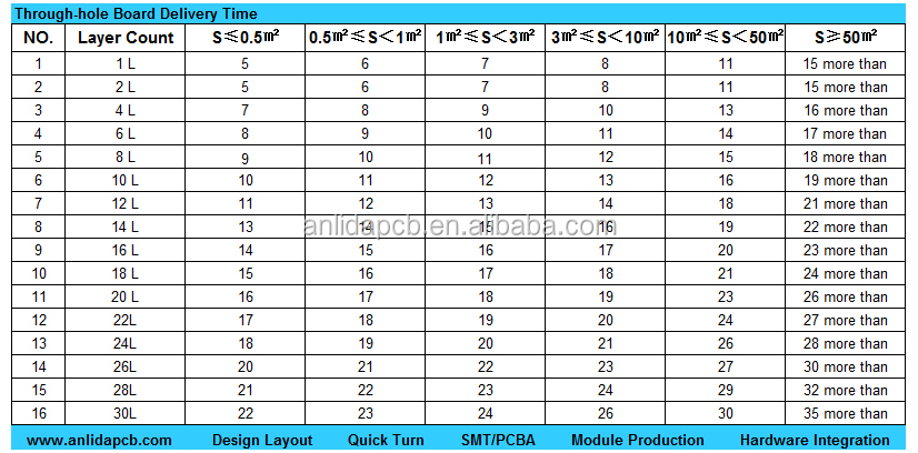
Production lead time:

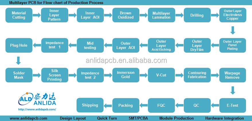
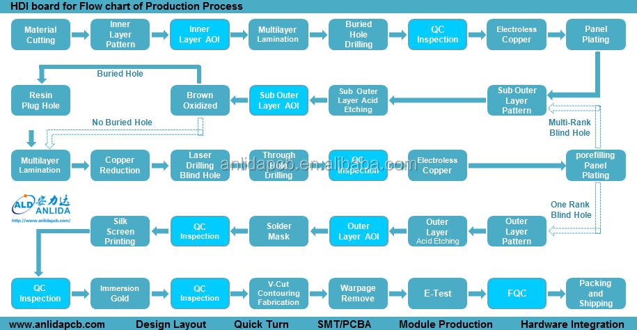
flow chart:
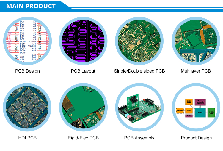
main products
VIEW MORE
You may like
-
Manufacturing custom design multi -layer HDI PCB and PCBA assembly plants for medical equipment for medical equipment

-
One Stop PCB Service Printed Circuit Factory Custom Multilayer PCBA Board All PCB Assembly and Manufacturing

-
Multilayer PCB Assembly Manufacturer ShenZhen Electronics SMT PCBA Factory

-
Shenzhen Customize PCB PCB Circuit Multilayer Pcb Manufacturer

-
Manufacturer PCB Circuit Board Assembly Professional Customer Printing Prototyping Factory Multilayer PCB and PCBA

-
Electronics Factory Multilayer Printed Circuit Board Manufacturer OEM ODM PCBA PCB Manufacturer Offer Electronic PCB Design

-
Original brand new TP.MS358.PB801 4-core wifi network 32--50 inch universal three-in-one motherboard suitable for smart TV accessories

-
Support one stop service Oem Professional Pcba Drone Pcb Drone Pcba

-
Cem-1 94v0 pcb schematic circuit board design services

-
Wind source dual system swimming pool heat pump constant temperature controller CC395 CCYCKB001

Related Search
mp3 player pcb circuit board manufacturer
tv box 94v0 pcb circuit board manufacturers
pcb circuit boards
flexible printed circuit boards manufacturers
pcb circuit boards led
mobile phone pcb circuit board suppliers
smd led pcb circuit board
circuit boards pcb manufacturing
4 layer multilayer multilayer pcb for emmc pcb
pcb board manufactures


