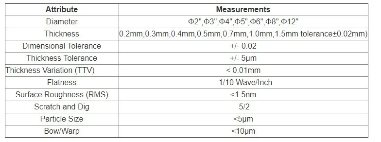
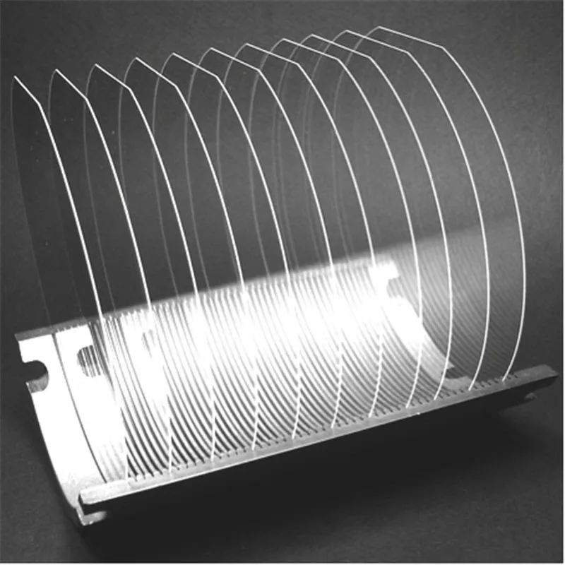
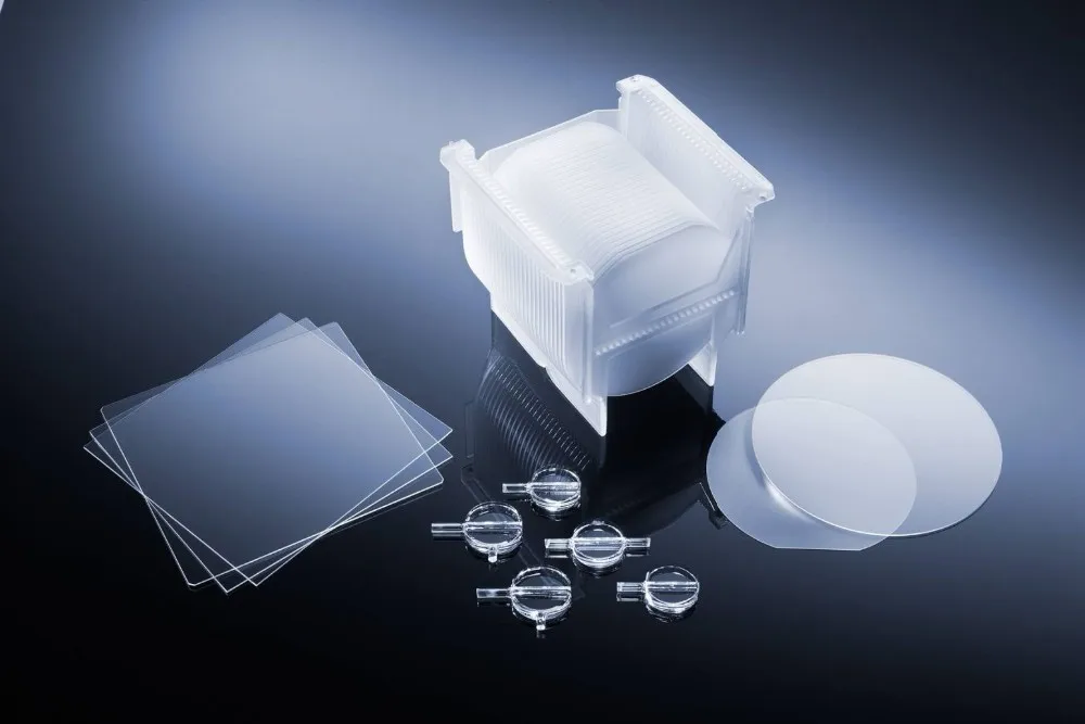
0.5mm 0.7mm 1.0mm thickness Borofloat33,borosilicate glass wafer for electrode patterning
-
Supplier: Xinyu Tking Glass Co., Ltd. -
Region: Jiangxi, China -
Contact: Ms Spring Lin -
Price: $1.00 / >=200 pieces -
Min. Order: 200 pieces
Product details
| Glass material2: | Soda lime glass, Borosilicate glass; | Glass material: | Borofloat33,Corning Eagle Xg , Quartz glass ,Corning Willow glass; |
| Thickness2: | 0.9mm 1.0mm 1.1mm 2.0mm 3mm 4mm 5mm 6mm 7mm 8mm; | Size: | 2'' 3'' 4'' 6'' 8'' 12''; |
| Packaging Detail: | Carton Box .; | Place of Origin: | Jiangxi China; |
| Light transmission: | 92%; | Polishing: | Both sides or one side polishing; |
| Payment Terms: | L/C,D/A,D/P,T/T; | Temperature resistant: | 550degree C; |
| Model Number: | Tk012; | Thcikness: | 0.1mm 0.2mm 0.3mm 0.5mm 0.7mm; |
| Brand Name: | Tking; |
Product Description
12'' Borosilicate 3.3 substrate glass wafers
WAFER SPECIFICATIONS
Tking produces wafers to all SEMI Standards including dimensional, flat and notch specifications. In addition, we offer custom specifications designed to your unique needs including, alignment marks, holes, pockets, edge profile, thickness, flatness, surface quality, cleanliness or any other details critical to your application. We also offer these wafers in a broad array of materials including Borosilicate, Aluminosilicate, Fused Silica (instead of quartz), Quartz and Soda Lime.
The following describes the versatility within several of our key processes. For full details on the process, please contact us freely get more information.
WAFER FABRICATION PROCESS
Shape Cut
Thin sheets are scribed, thick sheets are water jetted and blocks are wire sawn to begin the process with a wafer "blank".
CNC Edge
Each wafer is individually edged on a Precision CNC Edge Grinding Station.
Lapping
As required, wafers are lapped to precise thickness or flatness.
Polishing
Double-side Commercial Polish removes subsurface damage and Super Polish creates a pristine finish.
Cleaning
We combine ultrasonics and megasonics on multiple cleaning lines which feed directly into a Class 100 Clean Room.
Inspection
In our Class 100 Optical Clean Room, we inspect to various quality levels under the appropriate lighting conditions.
Packaging
All wafers are packed in pre-cleaned containers, double bagged and vacuum sealed within the Class 100 Clean Room.
Detailed Images
Certifications
Contact us
Tel:86+13414986564
Skype : yinhuanspring
Sales manager:Spring Lin
.
VIEW MORE
You may like
-
Hot selling ATMEGA16U2-MU official version Mega2560 R3 development board CH340G with USB cable suitable for Arduino projects

-
Inverter Control Car Trigger Board 193209-A03 193209-A06 193209-A08 74106-421-52

-
Original brand new fan K3G175-CF19-12

-
Semiconductor Refrigerator TEC1-12706 40*40 CPU Electronic Refrigerator Water Dispenser Radiator

-
Cooling Computer Components 12706 Peltier Thermoelectric Cooling Semiconductor Cooling System

-
Thermoelectric cooler Peltier 30*30mm TES1-12701 TES1-12702 TES1-12703 TES1-12704 TES1-12706

-
144W 12V Peltier Cooler Semiconductor Air Conditioner Cooling System DIY Kit

-
The power generation module of the generator with the thermoelectric Sebeck effect

-
DC 12V 288W Semiconductor Thermoelectric Peltier Cooler DIY Kits

-
2 inch diameter silicon wafer direction 100

Other Products
-
 $2.00 / piece
 -
 $1.50 / piece
 -
 $8.00 / piece
 -
 $7500.00 / set
 -
 $10.00 / piece
 -
 $10.00 / piece
 -
 $1.50 / piece
 -
 $8.00 / piece


