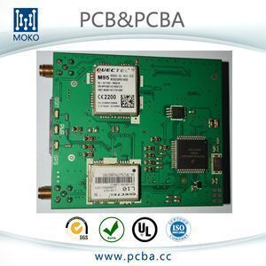
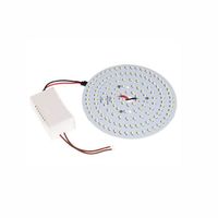
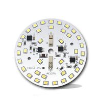
EMS quectel gsm m95 module pcb assembly
-
Supplier: Shenzhen Moko Technology Ltd. -
Region: Guangdong, China -
Contact: Ms Lara Huang -
Price: $0.10 /piece -
Min. Order: 1 piece
| Item: | wifi PCBA; | Standard: | IPC-A-610D; |
| Copper Thickness: | 1oz; | Base Material: | fr4; |
| Tolerance of finished panel: | ±10%; | Min. Line Width: | 0.1mm; |
| Max Panel size: | 800*508mm; | Surface Finishing: | Hasl lead free; |
| Board Thickness: | 1.6mm; | Impedence control and tolerance: | 50Ω±10%; |
| Place of Origin: | Guangdong China; | Min. Hole Size: | 0.25mm; |
| Service type: | One-stop turnkey service; | PCBA QC: | X-ray,AOI Test,Functional test; |
| Board finished thickness: | 0.2-4.0mm; | Wrap and twist: | ≤0.5%; |
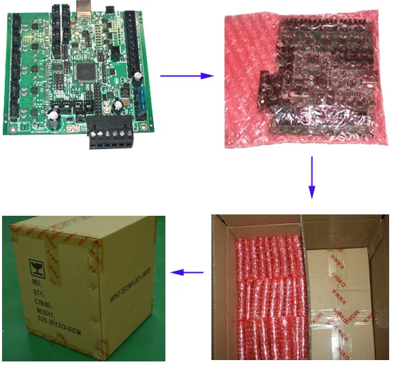
| Brand Name: | MOKO; | Packaging Detail: | Inner packing:Vacuum Package. Outer packing:High Quality Carton Box; |
| Min. Line Spacing: | 0.1mm; | Model Number: | MK60912BJ04; |
| Surface Treating Process of Inner: | Brown Oxide; | Port: | Shenzhen or Hong Komg; |
| Supply Ability: | 1000 Square Meter/Square Meters per Day fast lead time; | Payment Terms: | L/C,D/A,D/P,T/T,Western Union,MoneyGram,Escrow, PayPal; |
EMS quectel gsm m95 module pcb assembly
Welcome to Shenzhen MOKO
Shenzhen MOKO is an OEM one-stop electronic pcb and pcb assembly manufacturer
MOKO PCB&PCBA Contract Manufacturing Services Including as Belows:
v Fast PCB Fabrication for Samples and Mass Production
v Electronic Components Sourcing Services
v PCBA Assembly Services:SMT,DIP,BGA...
v Function Test
v Stencil,Cable and Enclosure Assembly
v Reverse engineering service
v Standard Packing and On time Delivery

Main Products Application:
v Household Appliances
v Medical Products
v Automotive Products
v Industrial Products
v Communication Products(AVL/GPS/GSM Devices)
v Consumer Electronics

MOKO service including:
1.PCB fabrication.
2.Turnkey PCBA:PCB+components+SMT and through-hole assembly+enclosure molding&housing.
3.PCB clone:reverse engineering,with all compoents compeleted.
Our advantages:
1.Free programming and free functional test,free package.
2.High quality:IPC-A-610E standard,E-test,X-ray,AOI test,QC,100% functional test.
3.Professional service.ISO SMT adn through hole assembly,over 10 years experience.
4.Certification for electronics:UL,94-V0,CE,SGS,FCC,Rohs,ISO9001:2008,ISO14001
5.Warranty period for PCBA:2 years.
PCB Board Processing Capability:
| 1 | Layers | Single Sided,2 to 18 Layer |
| 2 | Board material type | FR4,CEM-1,CEM-3,ceramic substrate board, aluminum based board, high-Tg, Rogers and more |
| 3 | Compound material lamination | 4 to 6 layers |
| 4 | Maximum dimension | 610 x 1,100mm |
| 5 | Dimension tolerance | ±0.13mm |
| 6 | Board thickness coverage | 0.2 to 6.00mm |
| 7 | Board thickness tolerance | ±10% |
| 8 | DK thickness | 0.076 to 6.00mm |
| 9 | Minimum line width | 0.10mm |
| 10 | Minimum line space | 0.10mm |
| 11 | Outer layer copper thickness | 8.75 to 175µm |
| 12 | Inner layer copper thickness | 17.5 to 175µm |
| 13 | Drilling hole diameter (mechanical drill) | 0.25 to 6.00mm |
| 14 | Finished hole diameter (mechanical drill) | 0.20 to 6.00mm |
| 15 | Hole diameter tolerance (mechanical drill) | 0.05mm |
| 16 | Hole position tolerance (mechanical drill) | 0.075mm |
| 17 | Laser drill hole size | 0.10mm |
| 18 | Board thickness and hole diameter ratio | 10:1 |
| 19 | Solder mask type | Green, Yellow, Black, Purple, Blue, White and Red |
| 20 | Minimum solder mask | Ø0.10mm |
| 21 | Minimum size of solder mask separation ring | 0.05mm |
| 22 | Solder mask oil plug hole diameter | 0.25 to 0.60mm |
| 23 | Impedance control tolerance | ±10% |
| 24 | Surface finish | Hot air level, ENIG, immersion silver, gold plating, immersion tin and gold finger |
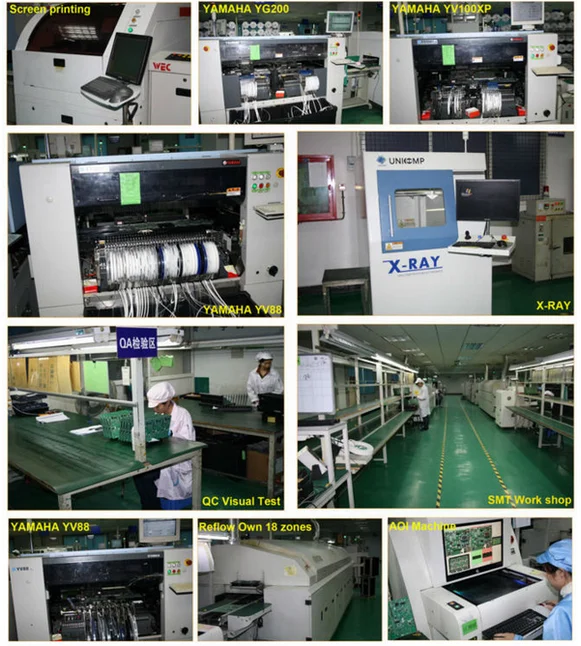
MOKO TECHNOLOGY LTD was founded in 2001, located in Shenzhen. We mainly offer Electronics Assembly Service. From our ISO9001:2008 certified factory, we turn out up to 10000 square meter of PCBs and 400000 PCBAs monthly. For assembly, utilizing 8 high-speed SMT lines from Yamaha and Sony, to meet customers' need.
MOKO offer PCBA for kickstarters, engineering offices and global elctronic companies.
Our PCBA are apply for medical care devices; vending machine; GPS tracker; Smoke alarm; Food detector; Blood pressure instrument; fish finder; communication board and other fields.
Overview of Our Workshop:
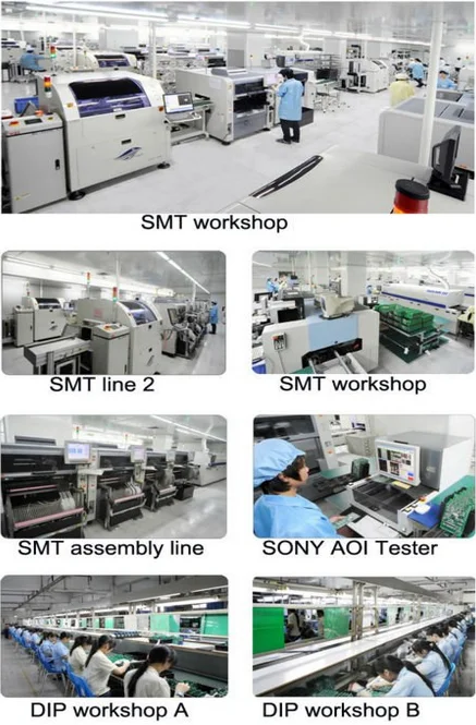
Advanced Machines:
Cooperation:


Shipping ways:
1.Small order: DHL,FEDEX,UPS,TNT,etc.
2.Larger order: By Sea.

PCB | Single/double side | 4 layer | 6 layer | Above 8 layer | HDI |
Sample lead time(Normal) | 5-6 | 6-7 | 7-8 | 10-12 | 15-20 |
Sample lead time(Fastest) | 48-72 hours | 5 | 6 | 6-7 | 12 |
Mass production lead time(First batch) | 7-9 | 10-12 | 13-15 | 16 | 20 |
PCB Assembly | PCB Fab+Components Sourcing+PCBA=20 days | ||||
Why us?
Quality
Our UL/Rohs standards insure quality assemblies from start to finish. Whether it's a simple custom product or a complex turnkey production run, Moko will adhere to the highest quality standards.
--------------------------------------------------------------------------------
Capable
Moko offers the latest in assembly capabilities and qualifications insuring that quality is built into every product we produce.
--------------------------------------------------------------------------------
Experience
When it comes to your build you want a partner you can depend on. Our management team has over 10years of combined industry knowledge. Our engineering team has over 7 years experience.
--------------------------------------------------------------------------------
Protecting your interests
Protecting your Intellectual Property is job one! Our staff of trained professionals are all working under a strict confidentiality contract and treat your important documentation as they would their own.
--------------------------------------------------------------------------------
Flexibility
We pride ourselves on our ability to custom tailor programs around our customers' needs. We take time to listen to your unique business needs and then set out to surpass them.
Should you have any further questions,please feel free to contact us!
-
Customized single sided round aluminum substrate, 12v led light circuit board factory

-
Support professional double-sided PCB design one-stop OEM service

-
Custom electronics contract manufacturing double sided pcb assembly

-
Wholesale Lighting Led Pcb Led Board Design Led Circuit Board 3535 5730 3w 5w 7w 9w 12w 15w 18w Smd LED Printed Circuit Board

-
Free Shipping 100% Original HDD PCB Logic Board 2060-800041-003 REV P1 Hard Drive Circuit Board 2060-800041-000 REV P1

-
best china kb 3151c fr-1 pcb with rohs long life

-
China Printed Circuit Board Automotive Mobile Medical PCBA Assembly PCB Design Service

-
RDS Electronics- Circular board PCB aluminum factory MCPCB 2835 LED SMD 5630 aluminum PCB

-
5G mobile phone FR4 PCB manufacturer Shenzhen

-
Shenzhen ODM double-sided PCB designer and Customized PCB Manufacturer


