Turnkey One Stop Electronics Printed Circuit Board PCB PCBA Assembly Component Sourcing
-
Supplier: Dalian Jy Electronics & Technology Co., Ltd. -
Region: Liaoning, China -
Contact: Mr Frank Zhu -
Price: $0.50 /piece -
Min. Order: 1 piece
| Flame resistance: | 94V-0; | Min. Line Width: | 0.08mm; |
| Brand Name: | JY; | Ring annulus: | Min 0.1mm; |
| Surface Finishing: | HASL,OSP,ENIG,Gold plating; | D/C: | JY; |
| Model Number: | JY PCB; | Place of Origin: | Liaoning China; |
| Impedance control: | ±5%; | Payment Terms: | L/C,D/A,D/P,T/T,Western Union,MoneyGram,PAYPAL ,ESCROW; |
| Finish Hole Size: | PTH ±0.003'' ,NPTH ±0.002"; | Min Plated Drills to Copper: | 0.25mm, 0.30mm; |
| Packaging Detail: | Packaging Detail: Inner Packing:Vacuum Packing/Plastic Bag Outer Packing:Standard Carton Packing; | Package: | Carton; |
| Port: | DALIAN PORT; | Service: | One Stop Service; |
| Supply Ability: | 600000 Square Meter/Square Meters per Month; | Certificate: | UL, SGS, RoSH, TS Certificate; |
| Application: | Communications Equipment; |
Electronics Printed Circuit Board PCB PCBA Assembly Component Sourcing
PCB Specification
| Product Name | Custom PCB Printed Circuit Board |
| Type | Rigid |
| Material | FR4, CEM1, CEM3, High Frequency Board, |
| Layer | 1,2,4,6...20Layer |
Shape | Rectangular, Round, Slots, Cutouts, Complex, Irregular |
| Cutting | Shear, V-score, Tab-routed |
| Board Thickness | 0.2-4mm, regular 1.6mm |
| Copper Thickness | 0.5-4oz, regular 1oz |
| Solder Mask | Green, Red, Blue, Yellow, etc. |
| Silk Screen | White, Black, etc. |
| Silk Screen Min Line Width | 0.006" or 0.15mm |
| Min Trace/Gap | 0.1mm or 4mils |
| Min Drill Hole Diameter | 0.01",0.25mm or 10mils |
| Surface Finish | HASL, ENIG, OSP, etc. |
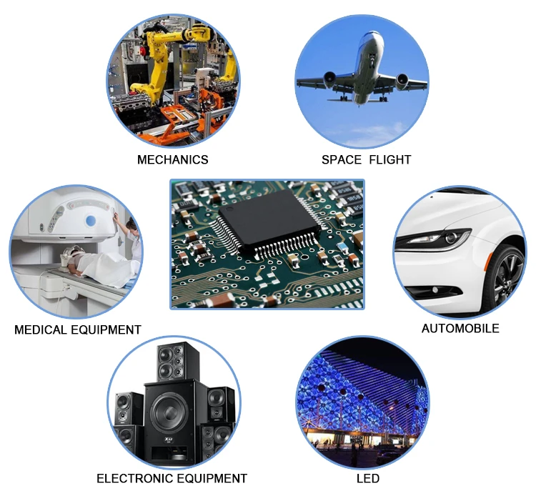
PCB Board we have produced are mainly used in the Industrial Control, Medical Treatment, Automobile area. All the products must meet ISO9001 UL CE etc. certification with high quality sodering for wires and no fingerprint.

| DHI PCB | HDI PCB Boards contain blind and/or buried vias and often contain microvias of .006 or less in diameter. They have a higher circuitry density than traditional circuit boards. |
| High TG PCB | The general TG plate is more than 130 degrees, the high TG is generally greater than 170 degrees, and the medium TG is more than 150 degrees. |
High Frequency PCB | RO4003C, RO4350B, Ro3003, Ro3010, and RT5880 etc with frequency typically in the range from 500MHz to 2GHz, products are applied to power devider,radar,satellite system, mobile phone reception base station and so on. |
Carbon Ink PCB | As carbon ink pcb has very good resistance value that will help supply good conductivity. Carbon ink pcb is widely used in automotive filed, medical electronics,communication equipment and so on. |
| Special Material PCB | Rogers4350,Rogers4003,Arlon 25FR,25N for Ceramic PCB powder filling, Rogers series, Taconic series,Arlon series,Nelco series ect for PTFE high frequency material. |
| Thick Copper PCB | Ensure that there is enough thick copper plating in the hole to ensure that the resistance is within the range of the process requirements. 70% of the circuit board to complete the use of 35um of copper foil thickness, some will use 70um , 105um ,140um copper thickness and so on. |
Main Products

Professional Electronic Bluetooth PCB Circuit Manufacturer
Certifications


Dalian JY Electronic Co., Ltd was established in 2002. We mainly offer High-Precision Single-Side, Double-Side, Multi-layer Printed Circuit Boards, LED Aluminium Printed Circuit Board, Customers Components Procurement and PCB Assembly (SMT) Business.
Now the production capacity of our factory has reached 600,000 square meters annually. And our products apply far and wide in many fields such as communication, computer, mobile phone, electronic equipment, and electrical appliance.
We established an assembly line in 2010, all the assembly machines were purchased from Panasonic, which can assemble the components of 0201. The production capacity of the PCBA is 2,000,000 points per day.

Drill is very important, so we have a perfect drill management area, and a machine 24 hours polished to ensure the quality of the drill bit.


PCBA Capability
| Item | Capability | Item | Capability |
Solder Paste Printing | Accuracy: ±0.025mm | Wave Soldering | |
| Max. speed: 150mm/sec | Nitrogen source: external | ||
| PCB max. area: 400*310mm | PCB max. size: 400*330mm | ||
| PCB thickness: 0.2-6mm | Temperature accuracy: ±1°C | ||
| SMT | Accuracy: ±0.03mm | Lead free compatible | |
| Speed: 0.17sec/pc | |||
| PCB max. area: 350*350mm | AOI | ||
Available part: 0201 chip to 35*35mm | Accuracy: ±0.0024mm | ||
| Accuracy: ±0.05mm | Speed: 5in² /sec (60FOV/sec) | ||
| Speed: 0.048sec/pc | PCB max. area:300*300mm | ||
PCB max. area: 350*350mm | Available component: 0201 chip and fine pitch | ||
Available part: 0402 chips to 14mm (H 12mm) | X-ray Inspection | ||
Minimum SMD resistor and capacitor: 0201 | BGA void (0.5mm distance between Ball) | ||
| Minimum BGA R-VTx: 0.15mm | Solderability inner shielding | ||
Reflow Soldering | Nitrogen source: external | BGA Rework | |
| PCB max. size: 400*330mm | Nitrogen source: NA | ||
| Temperature accuracy: ±4°C | PCB max. size: 350mm | ||
| Zones: 8 | Temperature accuracy: ±1°C | ||
| Lead free compatible | Lead free compatible |

Now we have been a factory which can provide one-stop service, from the PCB production, the components purchasing to the components assembled.

When we attended some Exhibition Show all around the world, such as USA, India, Japan, Thailand etc., our products attracted many people and they like our products and give high praise for our professional service. Thanks for their trust and we have already built long term business cooperation.
When the client visits our factory, all of them were satisfied with our workshop, they said "The factory is so clean, big and professional. Your machines, production line, and your team are amazing."

Our company is not only trying to give customers a good product but also pay attention to offering a complete and safe package. And here we prepare some personalized services for all the orders.
Common packaging:
PCB: Sealed bag, Anti-static bags, Suitable carton.
PCBA: Antistatic foam bags, Anti-static bags, Suitable carton.
Regular Cartons Specification.
| Regular Cartons Specification | No. Dimension (L*W*H) |
| Small Size | 33cm*28.5cm*18.5cm |
| Medium Size | 44.5cm*30cm*15cm |
| Big Size | 51.5cm*32.5cm*17.5cm |
Customized Cartons:
Carton outside according to the requirements of customers printed the name of the customer address, mark, the customer needs to specify the destination and other information.

PCB Fast Delivery
| Order Type / PCB Layers | 1/2-layer | 4-layer | 6-layer | Above 8-layer | HDI |
| First Batch Order | 7-9 days | 10-12 days | 13-15 days | 14-16 days | 20-22 days |
| Fast Sample Order | 48-72 hours | 5-7 days | 6-8 days | 6-7 days | 12-14 days |
| Normal Sample Order | 5-6 days | 6-7 days | 7-8 days | 10-12 days | 15-20 days |
-- FAQ --
- How to control products with high quality?
We ensuring products quality by IPC-610 F standard, The test will be done as customer’s requests. If any rejects during transportation, We will supply maintenance free of charge.
- What service can JY supply to the customer?
We can supply PCB, PCBA, Gerber design, Clone, OEM and ODM service.
- How does JY ensure customers' profit?
To protect customers' profit, we will sign NDA with customers and strictly abide by it.
- How long does it take to produce the PCB?
Generally 5-6 weeks for 5000 sets.
-
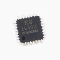
THJ new original EG8010 integrated circuit microcontroller IC inventory professional BOM supplier electronic components

-
TMS320VC33PGE150 LQFP-144 Digital Signal Processor and Controller DSP DSC BOM Integrated Circuits in Stock

-
KA3843 DIP8 best price.

-
AON6262E DFN5X6 New and Original IC Chip Support AON6262E BOM List

-
One-stop complete service electronic components, integrated circuits, capacitors, resistors, connectors, transistors,

-
CA-6928 Bluetooth Stereo Audio Module 5V 5.0BT Bluetooth Audio Board Small IC Bluetooth Chip

-
OEM series BOM supporting services Electronic components, ICS, diodes, transistors, transistors, capacitors, LEDs, etc.

-
Arduino UNO R3 Upgraded Learning Kit Latest RFID Starter Kit with Retail Box

-
Lefax A1000 Class A Power Amplifier Board

-
Mobile power module mobile power boost DIY18650 lithium battery digital display dual USB output charging board motherboard

Other Products
-
 $0.20 / piece
 -
 Original Mega 2560 R3 ATMEGA16U2-MU Board Photosensitive Resin 3D Printer Mega2560 for Arduinos Mega$0.70 / piece
 -
 $0.90 / piece
 -
 $0.70 / piece
 -
 $0.70 / piece
 -
 $0.50 / piece
 -
 $0.80 / piece


