Customized flexible Pcb manufacture in shenzhen,FPC
-
Supplier: Shenzhen Noeya Technology Co., Ltd. -
Region: Guangdong, China -
Contact: Ms Mary Hu -
Price: $0.10 /piece -
Min. Order: 1 piece
| Payment Terms: | L/C,T/T,Western Union,MoneyGram; | Brand Name: | Noeya; |
| Impedence Control Tolerance: | ±5%; | Finished copper thickness: | 1--6OZ; |
| Inner package: | vacuum package; | Board thickness tolerance: | ±10%; |
| Model Number: | FPC-1; | Port: | Shenzhen; |
| Min. Line Width: | 4mil; | Place of Origin: | Guangdong China (Mainland); |
| Shipping: | DHL UPS TNT Fedex; | Supply Ability: | 20000 Piece/Pieces per Month; |
| Plugging Vias Capability: | 0.2-0.8mm; | Board Thickness: | 0.05~1.0mm; |
| Base Material: | Polyimide,FR-4; | Packaging Detail: | Outer:high quality paper carton Inner:anti-static plastic/vacuum/bubble bags with desccant Middle paper board put in the carton as customer request; |
| Certificate: | ISO,UL, SGS and ROHS; | Copper Thickness: | 0.5oz , 1oz, 0.5oz~4oz; |
| Surface Finishing: | HASL Lead Free,OSP; | Min. Line Spacing: | 0.075mm; |
| Solder mask: | yellow; | Min. Hole Size: | 0.1mm; |
Customized flexible_rigid Pcb manufacture in shenzhen,FPC
Product Description
Product show:

Product parameters:
| Rigid board thickness: | 0.6mm |
| flex board thickness: | 0.13mm |
Size: | 77.8mm*73.2mm |
Layers: | 1-6 Layers |
Min. Line Width: | 0.05mm |
Min. Hole Size: | 0.15mm PTH |
Min. PTH Hole Ring: | 0.45mm |
Min. Gap between Cover Layer and Pad: | 0.1mm |
Min. Gap between Trace and Outline: | 0.2mm |
Trace Width Tolerance: | +/-0.03mm, W+/-30% |
Outline Tolerance: | +/-0.05mm L≤ 25mm |
Hole Size Tolerance: | +/-0.05mm |
Stiffener and Outline Tolerance: | +/-0.25mm |
Surface Treatment: | ENIG |
Manufacturing capacity:
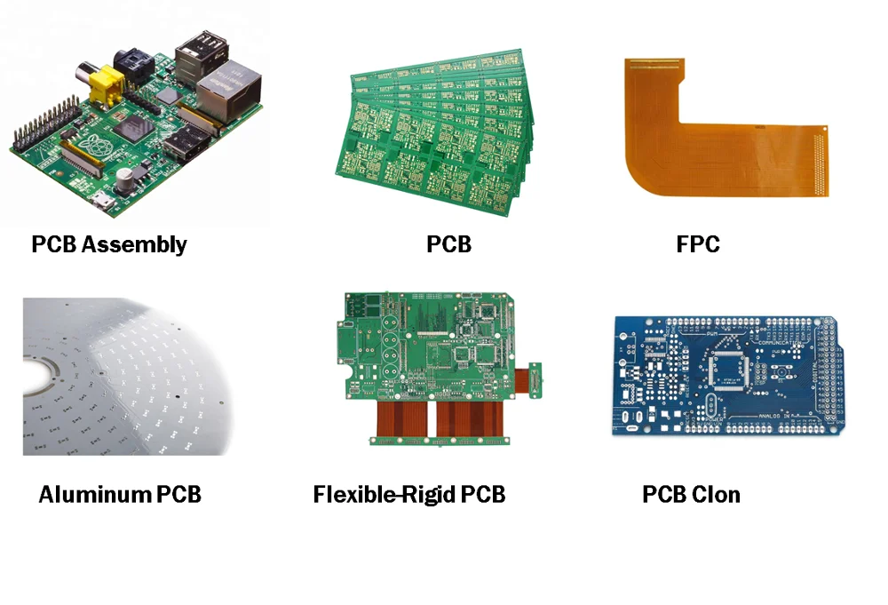
PCB
Item | Capability | |
1.Base Material | FR-1/FR-4 / High TG FR-4 / Lead free Materials (ROHS Compliant) / Halogen Free material /CEM-3/CEM-1/ /PTFE/ROGERS/ARLON/TACONIC FPC | |
2.Layers | 1-28 | |
3.Finised inner/outer copper thickness | 1-6OZ | |
4.Finished board thickness | 0.2-7.0mm | |
Tolerance | Board thickness≤1.0mm: +/-0.1mm 1 Board thickness>2.0mm: +/-8% | |
5.Max panel size | ≤2sidesPCB: 600*1500mm Multilayer PCB: 500*1200mm | |
6.Min conductor line width/spacing | Inner layers: ≥3/3mil Outer layers: ≥3.5/3.5mil | |
7.Min hole size | Mechanical hole: 0.15mm Laser hole: 0.1mm | |
Drilling precision: first drilling | First drilling: 1mil Second drilling: 4mil | |
8.Warpage | Board thickness≤0.79mm: β≤1.0% 0.80≤Board thickness≤2.4mm: β≤0.7% Board thickness≥2.5mm: β≤0.5% | |
9.Controlled Impedance | +/-5% | |
10. Aspect Ratio | 15:1 | |
11.Min welding ring | 4mil | |
12.Min solder mask bridge | ≥0.08mm | |
13.Plugging vias capability | 0.2-0.8mm | |
14. Hole tolerance | PTH: +/-3mil NPTH: +/-2mil | |
15.Outline profile | Rout/ V-cut/ Bridge/ Stamp hole | |
16.Surface treatment | OSP: 0.5-0.5um HASL: 2-40um Lead free HASL: 2-40um ENIG: Au 1-10U’’ ENEPIG: PB 2-5U’’/ Au 1-8U’’ Immersion Tin:0.8-1.2um Immersion silver: 0.1-1.2um Peelable blue mask Carbon ink Gold plating: Au 1-150U’’ | |
17.Solder mask | Green,Black,White,Blue,Red,Yellow,etc. | |
18.Silkscreen | Black,White,Blue,Red,Yellow,etc. | |
19. E-testing pass percent | 97% pass for the first time,+/-2%(tolerance) | |
FQC-Physical Lab: Reliability tests | ||
20.Certificate | UL,SGS,ROHS,ISO/TS16949,ISO14001:2004 | |
PCB ASSEMBLY
| Quantity | Prototype&Low Volume PCB Assembly,from 1 Board to 250,is specialty,or up to 1000 |
| Type of Assembly | SMT,Thru-hole |
| Solder Type | Water Soluble Solder Paste,Leaded and Lead-Free |
| Components | Passive Down to 0201 size BGA and VFBGA Leadless Chip Carriers/CSP Double-sided SMT Assembly Fine Pitch to 0.8mils BGA Repair and Reball Part Removal and Replacement |
| Bare Board Size | Smallest:0.25*0.25 inches Largest:20*20 inches |
| File Formate | Bill of Materials Gerber files Pick-N-Place file |
| Types of Service | Turn-key,partial turn-key or consignment |
| Component packaging | Cut Tape,Tube,Reels,Loose Parts |
| Turn Time | Same day service to 15 days service |
| Testing | Flying Probe Test,X-ray Inspection AOI Test |
High quality PCBA components procurement:
Quality international suppliers
For more than ten years, Noeya has been focusing on the pursuit of high quality, adopting international high-quality electronic components to pursue the production of higher quality products, at the same time providing better services, and has accumulated a number of excellent suppliers, such as Digi-key,Element,MOUSER, AVNET,WPI,FLEXTRONICS etc.
Quality domestic suppliers
The excellent domestic electronic component suppliers are also in the storage of Noeya, and we cannot tolerate any negligence in PCBA component quality.SIM, CZT, FENGHUA ADVANCED are excellent suppliers that have cooperated with us for many years.

Testing process:

Our services:


Company information

Noeya Technology Co., Ltd is a professional PCB manufacturer in China, Shenzhen. With 15 years of development,Noeya turns into a experienced manufacturer of HDI PCB, with production capability 35,000 square meters.
Noeya is providing high quality bare PCB and PCB assembly service,including components sourcing, function test, conformal coating and complete assembly for clients all over the world.
We can make:
1)1-28 layers PCB board
2)HDI Blind&Buried via multilayers PCB board
3)High frequency special material base PCB board, like Rogers, Taconic, Arlon, etc. 4)Thick copper Technology, impedance control standard
5)Assembly Processing: SMT, COB, THT
6)Testing Methods: Flying Probe Test, X-ray, ICT, AOI, FCTfactory direct
We provide 7days 24hours on-line professional Pre-sale, Selling and After-Sale service to solve any question about the order. Any time, any requirement will get Prompt Reply from our friendly support staff.
Access to view more...

Our main market is Europe, north USA,Australia, South America, Africa and Asia. we will put much more effort to build connection with more customers in more area. All we want to do, is to connect the world by our products, to share the Value, Happiness and Achievement with more customers.

Our Certification:
We have ISO/TS16949: 2000, ISO14001: 2004, UL, SGS, CE&RoHS report. We can provide the report of raw material based on customer’s requirement.


Application Scenarios:
Our products main application area is: Medical Instrumentation, Telecommunication
apparatus, industry power, Automotive, Liquid crystal module, Peripherals, Computing & storage, Consumer, Networking, satellite receiver (DVB), worker person who accuse of Hi-Tech trade is it produce and design the technological service to offer.

Packing:
As for packing, in order to avoid damage of products in international transportation as far as possible, we use high-quality cartons for outer packing and anti-static plastic/vacuum/bubble bag with dust collector for inner packing.

Shipment,order and payment:
Shipping information:
1.We will discuss the shipping details,and choosed the best option,and help customer shipping.
2.We also accept the pick up from our company by carrier,who cooperated with our customers and got a authorization from our customers.
3.Generally we will use air freight such as DHL,UPS,EMS,FEDEX,TNT,If need to by send by sea,we can discuss together.for DHL,UPS,need about 3-4 days to delivery,Fedex,about2-3 days.
order and Payment:
How to order?
You have 3 ways to order to us ,
1.Order on line.You can place the order on line,written down all your requirements and give us gerber file and bom list to us.We will take care of your orders as soon as you order to us.
2.Order us via E-mails.Sending E-mails to us as soon as you have your gerberfile ang bom of PCB&PCBA,and we will make it true for you.
3.You can simply give us a phone call to order to us.
How to do the payment?
We can accept pay by T/T,Paypal,West union ,or Trade Assurance on alibaba.If you want to pay buy other method,please contact us.
FAQ:
What files required to get quotation from you?
For PCB quotation, please provide the Gerber data/files and indication of related technical requirements as well as any special requirement if you have.
For PCBA quotation, please provide Gerber data/ files and also BOM (bill of materials), and if you need us to do function test, please also provide the test instruction/procedure.
What is your testing policy and how you controle the quality?
For sample, usually tested by flying probe; for PCB Volume over 3 square meters, usually tested by fixture, this will be more faster. Due to there’s many steps to PCB production, we usually do inspection after every step.
Do you have any minimum order quantity (MOQ) requirement?
No, we do not have MOQ requirement, we can support your projects starting from prototypes to mass productions.
Are my design files safe when I submit them to you for manufacturing?
Any customer’s file will be protected very well here in our factory and we will not let any third party know. We can sign NDA with you.
I only have the pcb sample, not pcb file, can you produce it for me?
Yes, we can copy file based on your sample, this file names gerber, and production then is accorded to gerber file.

-
Original FPC Flat Avh-x7780tv Avh X 7780 DVD TV Cable

-
EXW spot price avh x7550 7550 ced755 750 DVD FPC flat cable

-
Manufacturer specializing in the production of single and double FPC multi-layer circuit boards

-
48CM Mini Micro Nano SIM Card Extension FPC Cable

-
OEM fpc High Flex PCB Electronic Card PCB Circuit Board One Stop Service Flex PCB Manufacturer

-
FPC Aluminum UAV Controller Board Circuit Power Multilayer Accessory Factory Integrated Circuit

-
Manufacturer makes FPC online data entry works Ps5 Remapper flexible circuit LCD screen fpc Fpc double sided pcb cable

-
FPC processing factory flex pcb RoHS flexible circuit board FPC flex PCB

-
High temperature resistant custom PET flexible transparent FPC

-
Easy remapper soldered Remap Board fpc cable for PS5 Dual Sense BDM-010 Playstation 5 paddle ps5 smart

Other Products
-
 $0.50 / piece


